Loading...
Searching...
No Matches
SoM Power
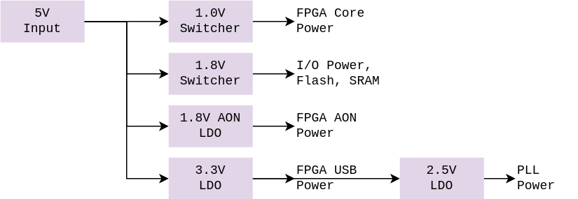
The SoM uses a single source of power at 5V, and exports several power rails at lower voltage using LDO and Buck converters.

The SoM supports turning all power rails off, except a single Always ON (AON) rail, only powering one power domain of the FPGA.
This allows staying in a deep sleep state until custom logic wakes the SoM.
Hardware integration of Power Rail
The SoM generates various voltage level useable by the user design within the current capability of the LDOs and buck converters.
| Name | Voltage | Current | EN pin | Type | Derived from |
|---|---|---|---|---|---|
| P5V | 5.0 V | max N/A | no | Input power | - |
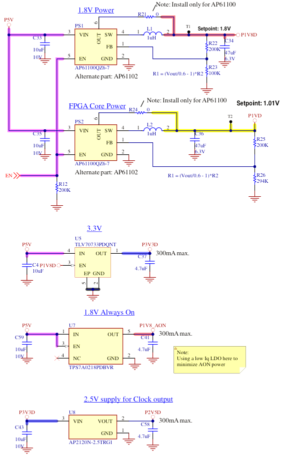
| P3V3D | 3.3 V | max N/A | yes | Output power | P5V with TLV707 |
| P2V5D | 2.5 V | max N/A | yes | Output power | P3V3D with AP2120N |
| P1V8D | 1.8 V | max N/A | yes | Output power | P5V with AP61102 |
| P1V8_AON | 1.8 V | max N/A | no | Output power | P5V with TPS7A021 |
| P1VD | 1.0 V | max N/A | yes | Internal | P5V with AP61102 |
- P5V: The only input power supply rail, typically coming from the power pins of the USB connector.
- P3V3D: Required by the FPGA, not used for any signal. Reused for deriving the 2.5V power rail out of it.
- P2V5D: Required for the Si5351 clock, not used for any signal.
- P1V8D: Required by the Flash and SRAM chips. If reused at the outside, this sets the I/O voltage level for these pins too.
- P1V8_AON: Required by the Always-On power domain, which stays on even when EN is low. Only for the FPGA to wake-up the rest.
- P1VD: Drawing most of the current to power the FPGA core. Not available to the outside.
Hardware integration of I/O voltage levels
The SoM allows to provide external reference voltages, directly applied to the FPGA I/O banks, thanks to 3 different pins used for different purposes at different supported ranges:
| Bank | Voltage Supply | Pins |
|---|---|---|
| USB VBUS | From SoM at 5.0 V | USB3 SSTX+/- SSRX+/-, USB2 D+/-, REFCLK, EN |
| Bank 0 | From SoM at 1.8 V | GPIOs, Flash/SRAM, PROGN, AON in/out |
| Bank 1 | 1.2 V to 3.3 V | GPIOs, JTAG, I2C |
| Bank 2 | 1.2 V to 1.8 V | Connectivity SoM variant differential pairs |
| Bank 3 | 1.2 V to 1.8 V | 6 differential pairs |
RTL integration
TODO: Describe the GPIO controller pin in use.
Zephyr integration
TODO: Describe the pinctrl DeviceTree integration.
Parts featured
- Diodes AP61102 buck converter
- Diodes AP2120N LDO
- Texas Instrument TLV707 LDO
- Texas Instrument TPS7A02 nanopower LDO
