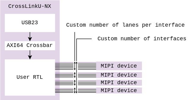
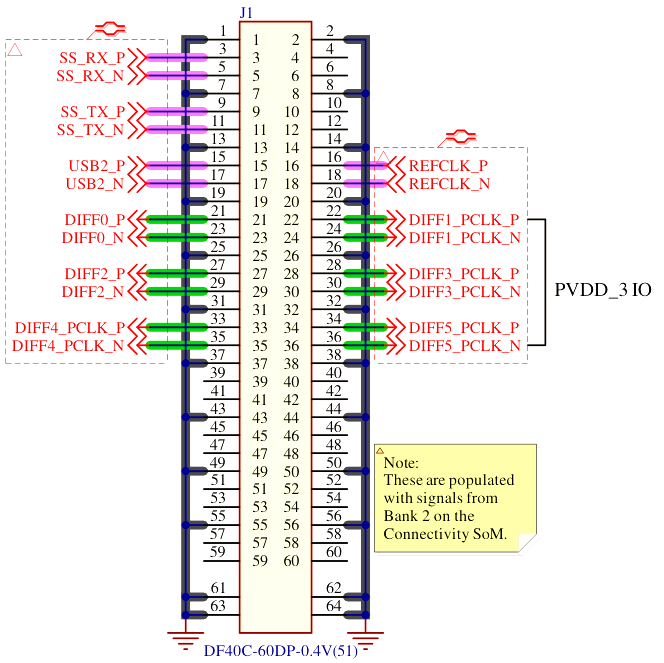
The differential pairs of the CrossLinkU-NX FPGA can be combined together into MIPI interfaces. These MIPI image signals can further be processed by the FPGA and be transferred through to USB 5 Gbit/s or another interface of any kind.

On the Compute SoM variant, some differential pairs are used for the external RAM, absent from the Connectivity SoM variant, leading to 6 or 14 differential pairs available.
Hardware integration
The MIPI pins are capable of 1.2 Gbit/s I/O in differential mode.
Each MIPI interface can have more or less differential pairs for the data lanes, and always one dedicated pair for the associated clock signal.
Connectivity SoM Lanes and Clocks (14 pairs available):
| 1L + 1C | 2L + 1C | 4L + 1C | Total |
|---|---|---|---|
| 1x | 2x | 13 | |
| 2x | 2x | 14 | |
| 3x | 1x | 14 | |
| 4x | 1x | 13 | |
| 1x | 2x | 1x | 13 |
| 1x | 4x | 14 | |
| 7x | 14 |
Compute SoM Lanes and Clocks (6 pairs available, others used by the RAM):
| 1L + 1C | 2L + 1C | 4L + 1C | Total |
|---|---|---|---|
| 1x | 5 | ||
| 2x | 6 | ||
| 1x | 1x | 5 | |
| 3x | 6 |
RTL integration
TODO: describe the FIFO interfaces available to feed the data from MIPI into USB
TODO: describe the MIPI data pipeline once released.
Zephyr integration
TODO: evoke the UVC configuration possible/required to do once UVC is there
Parts featured
- Lattice Semiconductor LIFCL-33U-8CTG104CAS FPGA (search for 33U in this page).
